

Understanding Of Fermi Level Pinning At Metal Germanium Interface Based On Semiconductor Structure Iopscience

Fermi Level Pinning By Defects In Hfo2 Metal Gate Stacks Applied Physics Letters Vol 91 No 13

Fermi Level Pinning And Hf Si Bonds At Hfo2 Polycrystalline Silicon Gate Electrode Interfaces Applied Physics Letters Vol 86 No 1

Bistable Fermi Level Pinning And Surface Photovoltage In Gan Sciencedirect

Van Der Waals Metal Semiconductor Junction Weak Fermi Level Pinning Enables Effective Tuning Of Schottky Barrier

Chemically Induced Fermi Level Pinning Effects Of High K Dielectrics On Graphene Scientific Reports

Fermi Level Pinning Explained A M S Contact Where The Fermi Level Is Download Scientific Diagram

A Fermi Level Pinning Free 1d Electrical Contact At The Intrinsic 2d Mos2 Metal Junction Yang 2019 Advanced Materials Wiley Online Library

Metal Semiconductor Junction Wikipedia
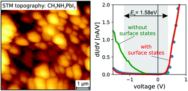
Fermi Level Pinning In Methylammonium Lead Iodide Perovskites Nanoscale Rsc Publishing
2


